Electronic Characterization, Measurements, and Test Benches
The team has access to shared equipment with the Nanoelectronics technical platform and also possesses various tools for characterizing thin films obtained through growth or transfer. These tools enable preliminary electronic characterization of components after cleanroom processing, as well as sensor testing.
Optical Characterization
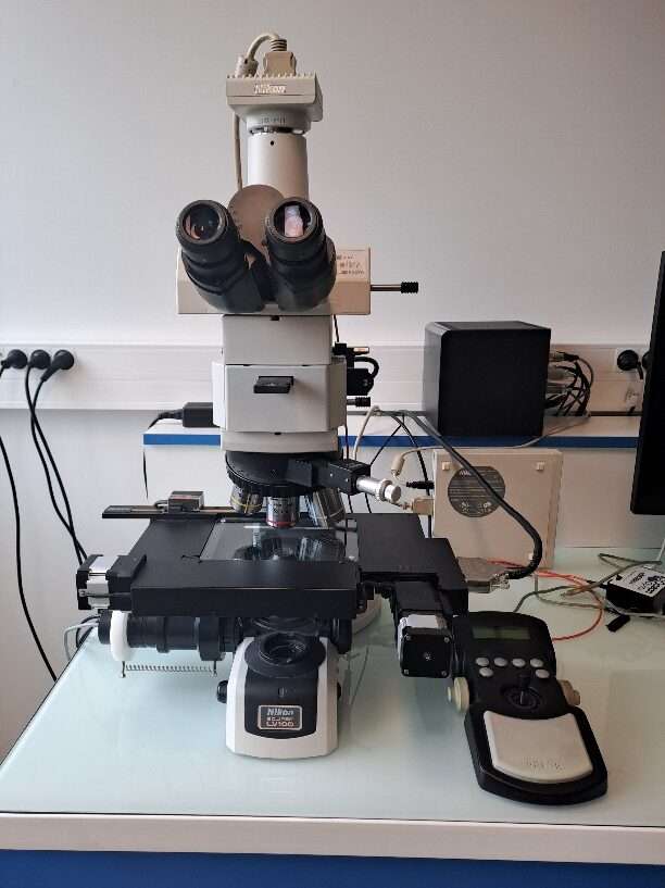
- A Nikon microscope equipped with a stable light source and a spectrometer, allowing sample observation and reflectometry measurements (particularly for thickness measurements).
- A commercial Horiba Raman spectrometer with a blue laser, primarily used for rapid characterization of graphene, other 2D materials, and SiC.
Basic and Advanced Electronic Characterization
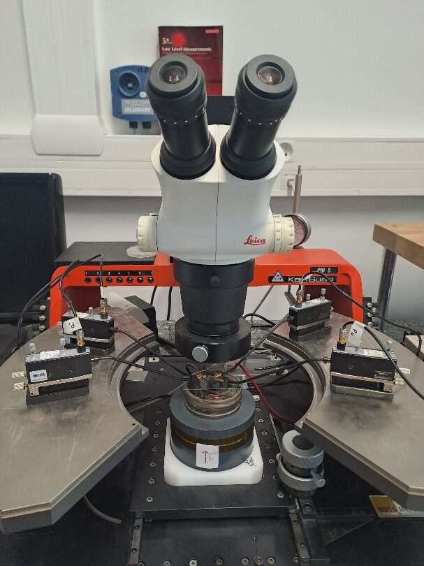
- A probe station with 4 probes and a small coil for preliminary air testing of components (contact resistance, doping, and mobility).
- A resistive coil (0.1 T) for low-noise measurements of magnetic field sensors.
- A low-frequency electronic noise measurement test bench.
- A low-concentration gas test bench (Air/CH₄/CO₂ – 10 ppm).
Additionally, the team has high hydrostatic pressure equipment (up to 2500 MPa) suitable for electronic transport studies.