Innovative materials – from growth to physical studies
Our research on wide-bandgap semiconductors focuses on two main families: nitrides and silicon carbide.
- Gallium nitride (GaN)-based structures: Our work investigates the structural, optical, and electrical properties of these materials and their associated electronic components. This research is conducted in collaboration with Unipress (https://www.unipress.waw.pl/) and the LabEX GANEXT (http://www.ganex.fr/).
- Silicon carbide (SiC): Recent efforts have concentrated on vanadium doping, particularly within the framework of the ANR Vanasic project.
Regarding graphene, our growth methods—sublimation on SiC and chemical vapor deposition (CVD) on copper—aim to produce high-quality, low-doped monolayers.
- Graphene on copper: This activity is carried out in long-standing collaboration with Annealsys, primarily for sensor applications (gas sensors and aqueous pollutant sensors).
- Graphene on SiC: This research is supported by several ANR projects, including MIGRASENS, SuperZiC, and VanaSiC.
- Exfoliated and encapsulated graphene: This activity is dedicated to more fundamental studies, as well as the development of tests sensors.
Beyond graphene, the team also explores other 2D materials, such as transition metal dichalcogenides (TMDs) like MoS₂. Our innovation lies in mastering the synthesis of large-area TMD monolayers to enable new applications.
All material research projects are conducted in close collaboration with the SCBD team of the NANO axis.
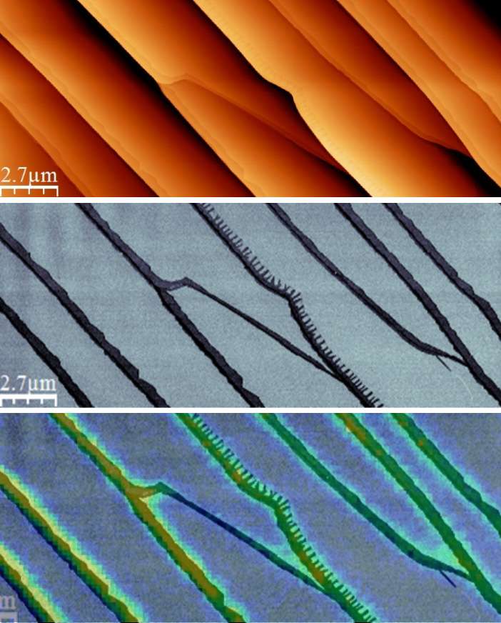
Graphene/SiC sample with µm-scale repositioning for multi-technique AFM and Raman analysis (from top to bottom: AFM topography, AFM phase, and superimposition of AFM and Raman mappings). Results obtained in collaboration with the SCBD team from the Nano axis [T. Wang https://theses.hal.science/tel-01946415v1]